
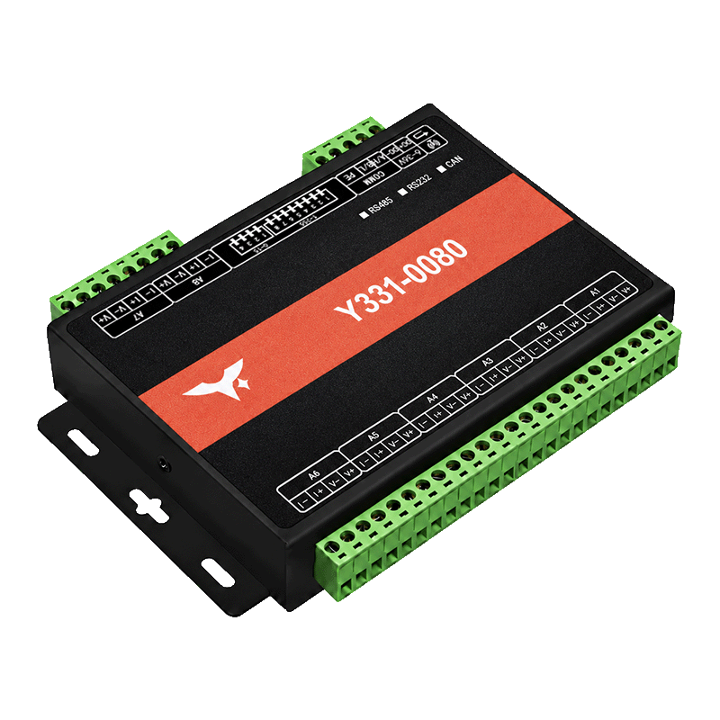
Appearance
Y331-0020/0040/0060/0080 Fully Isolated Multi-Range Analog Input Modules RS485 Technical Manual
Contents
- Overview
- Default Settings
- Modbus Register Map (Modbus Address Only)
- Command Examples (CRC Included)
- Parameter Configuration
- Analog Value Conversion
- Troubleshooting
1. Overview
Y331-0020/0040/0060/0080 modules acquire DC voltage and current signals through isolated input channels. The Specification lists signal ranges, electrical data, and ordering options.
Protocol profile: Use this manual with modules supplied with the register map below. Match the serial settings and input encoding to the supplied firmware profile before writing parameters. Section 6.4 explains milliamp conversion for voltage-encoded inputs.
| Model | DI | DO | AI | AO |
|---|---|---|---|---|
| Y331-0020 | 0 | 0 | 2 | 0 |
| Y331-0040 | 0 | 0 | 4 | 0 |
| Y331-0060 | 0 | 0 | 6 | 0 |
| Y331-0080 | 0 | 0 | 8 | 0 |
The four-position model code follows DI / DO / AI / AO, including zeros. The standard interface is isolated RS485; RS232 and isolated CAN are optional. RS232 wiring and settings, and CAN message definitions, require interface-specific documentation.
Frame format: [slave address][function code][data][CRC low][CRC high]
Command examples specify slave address 0x01. Replace it with the device address and recalculate the CRC. Send register addresses and data words high byte first, and CRC bytes low byte first.
2. Default Settings
| Parameter | Default |
|---|---|
| Slave address | 1 |
| Baud rate | 9600 bps |
| Data bits | 8 |
| Stop bits | 1 |
| Parity | None |
Active upload interval (0x0031) | 0; disabled |
Input data format (0x003A) | Read back 0x003A before decoding |
During commissioning, read 0x003A and check the active address and baud rate against the supplied register map and DIP-switch settings.
3. Modbus Register Map (Modbus Address Only)
Register addresses are zero-based protocol addresses. Registers hold unsigned 16-bit values. RO means read only; RW means read/write.
3.1 Analog Input (AI) - Function Code 0x04
| Channel | Modbus Address | Description | Unit | R/W |
|---|---|---|---|---|
| AI1 | 0x0000 | AI1 sampled value | V / A* | RO |
| AI2 | 0x0001 | AI2 sampled value | V / A* | RO |
| AI3 | 0x0002 | AI3 sampled value | V / A* | RO |
| AI4 | 0x0003 | AI4 sampled value | V / A* | RO |
| AI5 | 0x0004 | AI5 sampled value | V / A* | RO |
| AI6 | 0x0005 | AI6 sampled value | V / A* | RO |
| AI7 | 0x0006 | AI7 sampled value | V / A* | RO |
| AI8 | 0x0007 | AI8 sampled value | V / A* | RO |
*For milliamp inputs, use the encoding and sampling resistance specified for the supplied hardware; see Section 6.4.
Each AI channel uses one register. Read only the fitted AI count in the model code: for example, AI1-AI4 on Y331-0040 and AI1-AI8 on Y331-0080.
3.2 Common Holding Registers (Parameters) - Function Code 0x03/0x06/0x10
| Modbus Address | Parameter | Bytes | R/W | Range / Enum | Default |
|---|---|---|---|---|---|
0x0031 | Active upload interval | 2 | RW | 0 disables upload; use the interval unit in the supplied firmware profile | 0 |
0x0032 | Slave address | 2 | RW | 1-255 | 1 |
0x0033 | Baud-rate code | 2 | RW | 0-7; see Section 5.3 | 1 |
0x003A | Input data format | 2 | RW | 0-3; see Section 5.4 | Read back |
0x003D | Parity | 2 | RW | 0=none, 1=odd, 2=even | 0 |
4. Command Examples (CRC Included)
Send each request as hexadecimal bytes, including its CRC.
4.1 Read Analog Inputs
| Operation | Request (Hex) |
|---|---|
| Read AI1 | 01 04 00 00 00 01 31 CA |
| Read AI2 | 01 04 00 01 00 01 60 0A |
| Read AI3 | 01 04 00 02 00 01 90 0A |
| Read AI4 | 01 04 00 03 00 01 C1 CA |
| Read AI5 | 01 04 00 04 00 01 70 0B |
| Read AI6 | 01 04 00 05 00 01 21 CB |
| Read AI7 | 01 04 00 06 00 01 D1 CB |
| Read AI8 | 01 04 00 07 00 01 80 0B |
4.2 Read All Fitted Analog Inputs
| Operation | Request (Hex) |
|---|---|
| Y331-0020: read AI1-AI2 | 01 04 00 00 00 02 71 CB |
| Y331-0040: read AI1-AI4 | 01 04 00 00 00 04 F1 C9 |
| Y331-0060: read AI1-AI6 | 01 04 00 00 00 06 70 08 |
| Y331-0080: read AI1-AI8 | 01 04 00 00 00 08 F1 CC |
4.3 Interpret an AI1 Response
text
Request:  01 04 00 00 00 01 31 CA
Response: 01 04 02 03 E8 B9 8E
The returned word is 0x03E8, decimal 1000. With fixed three-decimal format and voltage encoding, it represents 1.000 V. For milliamp inputs, apply the hardware-specific conversion in Section 6.4.
4.4 Parameter Read/Write
| Operation | Request (Hex) |
|---|---|
Read slave address (0x0032) | 01 03 00 32 00 01 25 C5 |
| Write slave address = 2 | 01 06 00 32 00 02 A9 C4 |
Read baud-rate code (0x0033) | 01 03 00 33 00 01 74 05 |
| Write baud rate = 38400 bps (code 4) | 01 06 00 33 00 04 78 06 |
Read input data format (0x003A) | 01 03 00 3A 00 01 A4 07 |
| Write fixed three-decimal format (code 2) | 01 06 00 3A 00 02 28 06 |
Slave address, baud rate, parity, and input data format persist after power loss. Changes take effect after power cycling. Reconnect using the new serial settings.
5. Parameter Configuration
5.1 Wiring and First Connection
Mounting: Screw mounting. Secure the module to a cabinet backplate or another flat surface using the enclosure mounting slots before wiring.
| Group | Connection |
|---|---|
DC+ / DC- | 6-36 VDC supply positive / negative |
V+ / V- | Voltage input positive / negative for each channel |
I+ / I- | Current input positive / negative for each channel |
A/H / B/L | Use the interface-specific terminal drawing for pin assignments |
PE | Earth terminal; follow the model-specific drawing |
With power disconnected, check the ordered range and terminal labels. Use the matching voltage or current terminals. Connect voltage inputs across the source and current inputs in series with the measured circuit. Keep each channel's input return separate to preserve the isolation between channels.
Start with one module and one RS485 master using the settings from the firmware-specific documentation. Read AI1 and compare the decoded result with a known signal. Assign a unique address to each module on the bus.
5.2 Slave Address
Write a value from 1 to 255 to register 0x0032.
5.3 Serial Settings
Baud rate uses a 16-bit code at 0x0033.
| Baud-rate code | Baud rate (bps) |
|---|---|
| 0 | 4800 |
| 1 | 9600 |
| 2 | 14400 |
| 3 | 19200 |
| 4 | 38400 |
| 5 | 56000 |
| 6 | 57600 |
| 7 | 115200 |
Set parity at 0x003D: 0 = none, 1 = odd, 2 = even. Serial frames have 8 data bits and 1 stop bit.
5.4 Input Data Format
Set the decimal format at 0x003A:
| Code | Format |
|---|---|
| 0 | Variable decimal |
| 1 | Fixed two decimals |
| 2 | Fixed three decimals |
| 3 | Fixed four decimals |
Register 0x003A controls the value encoding, not the physical input range. The ordered hardware determines the signal range.
5.5 Active Upload Interval
Register 0x0031 controls active upload; 0 disables it. Set the interval using the unit in the supplied firmware profile. For a profile that uses 0.01 s per count, 200 gives 2 s. Keep upload disabled during initial polling.
5.6 Hardware Address and Baud Controls
Set the address and baud rate according to the supplied DIP-switch table. Follow its switch/register priority and reset procedure, then reconnect with the active settings.
6. Analog Value Conversion
6.1 Variable Decimal Input Format
For raw register value R, the ten-thousands digit sets the number of decimal places. The remaining four digits give the magnitude:
text
d = floor(R / 10000)
n = R % 10000
decoded value = n / 10^d
Example: R = 31000 gives d = 3, n = 1000, and a decoded value of 1.000.
6.2 Fixed Decimal Input Format
text
decoded value = R / 10^dThe value of d is 2, 3, or 4, as selected by register 0x003A. With fixed three-decimal format, R = 1000 gives 1.000.
Fixed four-decimal voltage encoding represents at most 6.5535 V in an unsigned 16-bit register. Select two- or three-decimal encoding for the full range of 0-10 V and 0-30 V inputs. Check the required precision for millivolt inputs against a known reference signal.
6.3 Voltage Inputs
The decoded input value is in volts. For example, 1.000 V equals 1000 mV.
6.4 Milliamp Inputs: 0-20 mA and 4-20 mA
For inputs that encode the voltage across a 249 Ω sampling resistor, convert the decoded voltage to current using the formulas below. Apply them only when the supplied firmware profile specifies this encoding and resistance:
text
current (A)  = decoded voltage (V) / 249
current (mA) = decoded voltage (V) × 1000 / 249
Example: 1.000 V / 249 Ω = 0.004016 A, approximately 4.016 mA. This example assumes the 249 Ω voltage encoding. Scale it separately to the transmitter's engineering range when required.
For a 4-20 mA transmitter whose endpoints are low and high:
text
engineering value = low + (current_mA - 4) × (high - low) / 166.5 Ampere Inputs: 0-2 A and 0-10 A
For firmware profiles that report ampere inputs in A, compare the decoded value with a known current during commissioning.
7. Troubleshooting
| Symptom | Cause | Solution |
|---|---|---|
| No response | Supply, wiring, or communication setting mismatch | Check supply, A/B polarity, address, baud rate, and parity |
| Response stops after configuration | Module and host settings differ | Power-cycle and reconnect using the new settings |
| Input value has the wrong scale | Incorrect decimal format | Read 0x003A and decode with the corresponding format |
| Milliamp value is incorrect | Conversion does not match the hardware | Use the encoding and sampling resistance specified for the hardware |
| Some channels cannot be read | Request exceeds the fitted AI count | Match the register count to the model |
LED Indicators
| Indicator | Function |
|---|---|
| PWR | Power indicator |
For troubleshooting assistance, email [email protected] with the full model, signal ranges, serial settings, request frame, and response frame.
- Manufacturer: Hunan YenGear Tech Co., Ltd.
- Email: [email protected]
- Website: www.yengear.com